Raspberry Pi Pico 2 W Pinout
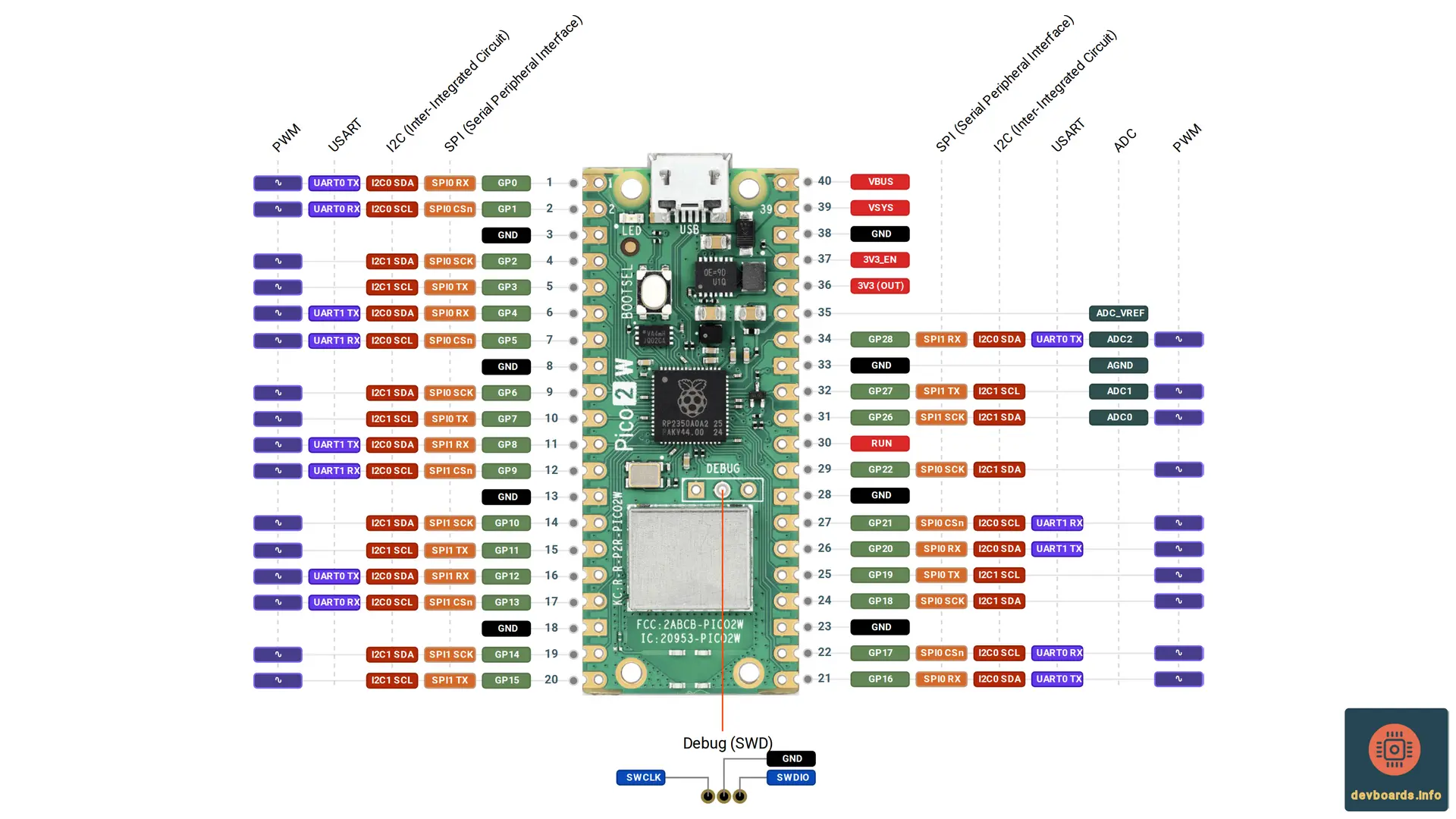
The Raspberry Pi Pico 2 W is the wireless member of the Raspberry Pi Pico 2 family. It combines the RP2350 microcontroller with an Infineon CYW43439 wireless chip, so the board gains single-band 2.4 GHz Wi-Fi and Bluetooth 5.2 on top of everything the Pico 2 offers. The Raspberry Pi Pico 2 W pinout and board layout are identical to those of the original Raspberry Pi Pico W, and the board keeps hardware and software compatibility with the first-generation Pico boards.
The microcontroller on this board is the RP2350A variant. It can run on either two Arm Cortex-M33 cores or two Hazard3 RISC-V cores, clocked at up to 150 MHz, and it comes with 520 kB of on-chip SRAM. Programs are stored in 4 MB of external QSPI flash and executed in place.
The RP2350 has 30 GPIO. The Pico 2 W routes 26 of them to its 40-pin edge connector as 3.3 V multi-function pins, three of which (GP26 to GP28) also work as 12-bit ADC inputs. The remaining four, GPIO23, GPIO24, GPIO25 and GPIO29, are used on the board itself to drive the wireless chip's SPI link and to measure the VSYS supply voltage.
Wireless communication runs over an SPI connection between the two chips. The CYW43439 also has three GPIO of its own that the board uses for housekeeping: one drives the on-board LED, one controls the power-save mode of the switch-mode power supply, and one senses whether USB power is present.
Key features of the Raspberry Pi Pico 2 W include:
- RP2350A microcontroller with dual Arm Cortex-M33 or dual Hazard3 RISC-V cores, up to 150 MHz
- 520 kB SRAM and 4 MB QSPI flash memory
- 26 multi-function 3.3 V GPIO pins, 3 of them ADC capable
- Wi-Fi 4 (802.11n), single-band 2.4 GHz, with WPA3 and SoftAP for up to 4 clients
- Bluetooth 5.2 with Bluetooth LE Central and Peripheral roles and Bluetooth Classic
- 2 × UART, 2 × SPI, 2 × I2C and 16 PWM channels
- 3 Programmable I/O (PIO) blocks with 12 state machines in total, plus an HSTX peripheral
- 12-bit, 500 ksps analog-to-digital converter
- USB 1.1 device and host support through a Micro USB B port
- On-board buck-boost power supply that accepts about 1.8 V to 5.5 V
- 3-pin Arm Serial Wire Debug (SWD) port
- Castellated edges, so the board can be soldered down as a surface-mount module
- Programmable in C/C++ with the Pico SDK, MicroPython, CircuitPython and the Arduino IDE
Raspberry Pi Pico 2 W Technical Specification
| Platform | |
|---|---|
| Manufacturer | Raspberry Pi |
| Processor | RP2350 |
| Processor Family | Arm Cortex-M33 |
| Clock Speed | 150 MHz |
| Flash Memory | 4 MB |
| SRAM | 520 KB |
| I/O | |
|---|---|
| Digital I/O | 26 |
| Analog Input | 3 |
| PWM | 16 |
| ADC Resolution | 4096 |
| Interrupts | 26 |
| Power | |
|---|---|
| Input Voltage | 5 V |
| I/O Voltage | 3.3 V |
| I/O Current | 12 mA |
| Communication Protocols | |
|---|---|
| I2C | 2x |
| SPI | 2x |
| UART | 2x |
| Connectivity | |
|---|---|
| USB Micro B | 1x USB 1.1 device or host |
| WiFi | 802.11n Provided by Infineon CYW43439 module WPA3, SoftAP with up to 4 clients |
| Bluetooth | 5.2 Provided by Infineon CYW43439 module Bluetooth LE Central and Peripheral roles, Bluetooth Classic |
| Peripherals | |
|---|---|
| Timer | 2x 64 bit |
| Watchdog Timer | 1 |
| Cryptography | Arm TrustZone for Cortex-M, signed boot, 8 kB OTP, SHA-256 acceleration, hardware TRNG |
| Debug/Trace | SWD |
| Dimensions | |
|---|---|
| Width | 21 mm |
| Length | 51 mm |
Raspberry Pi Pico 2 W Pin Headers and Components
The Pico 2 W keeps the familiar Pico footprint. Here is a walk through its physical features:
Dimensions
The board is a single-sided PCB measuring 51 mm × 21 mm and 1 mm thick. Four 2.1 mm drilled mounting holes allow it to be fixed to an enclosure or a carrier board.
Pin headers and castellations
The 40 user pins of the Raspberry Pi Pico 2 W pinout run along the two long edges on a 2.54 mm (0.1 inch) grid with 1 mm holes, so the board fits breadboards and stripboard once pin headers are soldered on. The board is one 0.1 inch pitch wider than a standard 40-pin DIP package. The same pins are castellated, which means the Pico 2 W can also be reflow-soldered directly onto another PCB as a module.
Micro USB port
The Micro USB B connector overhangs the top edge of the board and carries both power and data. It is a through-hole part for mechanical strength. When the board is used as a surface-mount module, SMT pads underneath the USB connector and the BOOTSEL button give access to those signals.
RP2350 microcontroller
The RP2350 is supported by a minimal set of external parts: a 4 MB QSPI flash chip, a 12 MHz crystal, the power supply and decoupling components, and the USB connector.
Infineon CYW43439 and antenna
The CYW43439 wireless chip feeds an on-board antenna licensed from Abracon (formerly ProAnt), located at the bottom edge of the board. The antenna cutout is 14 mm × 9 mm, and nothing should intrude into that space: metal under or near the antenna reduces both gain and bandwidth. For the best range, place the Pico 2 W at the edge of a carrier board and do not enclose it in metal. Adding grounded metal to the sides of the antenna can improve its bandwidth slightly.
BOOTSEL button
Holding the BOOTSEL button while the board powers up starts the USB mass-storage bootloader, which is how new firmware is copied onto the board without any other tools.
On-board LED
The user LED is not wired to an RP2350 pin. It is driven by WL_GPIO0 of the CYW43439, so it is switched through the wireless driver rather than as a normal GPIO.
Debug header (SWD)
A 3-pin Serial Wire Debug header sits near the middle of the board, below the microcontroller. On the Pico 2 W it is made of three castellated through-hole pads; the Pico 2 W with headers uses a small keyed 3-pin JST-style connector instead, which fits the Raspberry Pi Debug Probe directly.
Test points
Six test points, TP1 to TP6, expose the USB data lines, BOOTSEL and two of the wireless chip's GPIO. They are mainly useful when the board is soldered down as a module and the Micro USB port and button are not reachable.
Operating conditions
The recommended operating temperature range is -20 °C to 70 °C, including self-heating.
Powering Raspberry Pi Pico 2 W
The Pico 2 W is built around an RT6154 buck-boost switch-mode power supply (SMPS) that produces the 3.3 V rail for the RP2350 and its I/O. Because it can switch seamlessly between buck and boost operation, it keeps a stable 3.3 V output from any input between about 1.8 V and 5.5 V. That makes the board easy to run from USB, a bench supply, a single lithium-ion cell or three AA cells in series.
Micro USB port
Plugging in the Micro USB port is the simplest way to power the board. The USB voltage (VBUS) passes through a Schottky diode (D1) to become VSYS, the main system input, so VSYS sits one diode drop below the USB voltage. The recommended VBUS range is 5 V ± 10%.
VBUS pin
The VBUS pin (pin 40) in the Raspberry Pi Pico 2 W pinout is connected directly to the Micro USB supply. It is nominally 5 V when USB is connected and 0 V otherwise. If USB is the only power source, VBUS and VSYS can be shorted together to remove the diode drop, which improves efficiency and reduces ripple. When the Pico 2 W acts as a USB host, it must be powered by supplying 5 V to this pin.
The wireless chip's WL_GPIO2 monitors VBUS and reads high when USB power is present, so software can tell whether the board is running from USB or from another source.
VSYS pin
The VSYS pin (pin 39) in the Raspberry Pi Pico 2 W pinout is the main system input and accepts 1.8 V to 5.5 V. If the USB port is not used, a supply or battery can be connected to VSYS directly. To combine a second supply with USB, feed it into VSYS through another Schottky diode so the higher of the two voltages wins. A more efficient option is a P-channel MOSFET whose gate is controlled by VBUS, which disconnects the secondary source whenever USB is present; the datasheet suggests the Diodes DMG2305UX for most situations.
VSYS is also divided by three and connected to ADC channel 3 (GPIO29), which can serve as a simple battery voltage monitor. Because that pin is shared with the wireless SPI clock, VSYS can only be measured when no wireless SPI transaction is in progress.
3V3 pin
3V3 (pin 36) is the 3.3 V output of the SMPS that powers the RP2350 and its I/O. It can supply external circuits, but the available current depends on the RP2350 load and the VSYS voltage, so the datasheet recommends keeping the load on this pin under 300 mA.
3V3_EN pin
3V3_EN (pin 37) connects to the SMPS enable input and is pulled up to VSYS through a 100 kΩ resistor. Shorting it to ground turns off the 3.3 V supply, which also removes power from the RP2350 and puts the regulator into a low-power state.
RUN pin
RUN (pin 30) is the RP2350 enable pin. It has an on-chip pull-up of about 50 kΩ to 3.3 V; pulling it low resets the microcontroller.
SMPS power-save mode
WL_GPIO1 on the wireless chip drives the power-save (PS) pin of the SMPS. By default it is low, and the regulator runs in pulse frequency modulation (PFM) mode, which saves considerable power at light loads. Driving it high forces pulse width modulation (PWM) mode, which greatly reduces output ripple at light loads at the cost of much lower efficiency. Under heavy load the regulator runs in PWM mode regardless of the PS pin.
Battery charging
A power-path battery charger can be added by feeding VBUS into the charger input and connecting the charger output to VSYS through the P-channel MOSFET arrangement described above. Lithium-ion cells must have proper protection against over-discharge, over-charge, over-current and charging outside their allowed temperature range.
GND pins
Seven GND pins are spread along the headers to provide return paths and reduce electromagnetic interference and crosstalk. A separate AGND pin (pin 33) is the ground reference for the ADC-capable GPIO26 to GPIO29.
Raspberry Pi Pico 2 W Pinout and Peripherals
Every peripheral on the Pico 2 W comes from the RP2350, apart from the wireless interface, which is provided by the CYW43439. Here is what the board exposes:
Digital GPIO
The Raspberry Pi Pico 2 W pinout exposes 26 GPIO pins on the headers, all fixed at 3.3 V logic because they are powered from the on-board 3.3 V rail. GP0 to GP22 are digital-only, while GP26 to GP28 can be used as digital GPIO or as ADC inputs. GPIO 0 to 25 can safely receive up to 3.3 V even while the RP2350 is unpowered. The ADC-capable pins cannot: they have a reverse diode to the 3.3 V rail, so their input must not exceed 3.3 V plus about 300 mV, and voltage applied to them while the board is unpowered leaks into the supply.
Analog to Digital Converter (ADC)
The RP2350 has a 12-bit, 500 ksps ADC. Three channels, ADC0 to ADC2 on GP26 to GP28, are available on the headers, and ADC3 on GPIO29 measures VSYS/3. The ADC uses its own supply as a reference; on the Pico 2 W that supply (ADC_VREF) is derived from the 3.3 V rail through an RC filter (201 Ω into 2.2 µF). This introduces an offset of roughly 30 mV and lets some supply noise through. Accuracy can be improved by driving the SMPS into PWM mode during conversions, by using a second ADC channel tied to ground to measure the offset, or by connecting an external 3.0 V shunt reference such as the LM4040 to the ADC_VREF pin, which limits the input range to 0 V to 3.0 V.
UART
Two UART controllers are available. The Pico SDK board definition uses UART0 on GP0 (TX) and GP1 (RX) by default.
I2C
Two I2C controllers are available. The default I2C0 pins in the Pico SDK are GP4 (SDA) and GP5 (SCL).
SPI
Two SPI controllers are available. The SDK defaults for SPI0 are GP18 (SCK), GP19 (TX), GP16 (RX) and GP17 (CS).
PWM
The RP2350 provides 16 PWM channels, which can be routed to the GPIO pins for dimming LEDs, driving servos or controlling motor speed.
Programmable I/O (PIO)
Three PIO blocks with twelve state machines in total let you build flexible, high-speed I/O interfaces in software. They can emulate interfaces such as SD card and VGA that have no dedicated hardware peripheral. The RP2350 also includes an HSTX peripheral.
Timers
The RP2350 provides two hardware timers with four alarms each and an always-on (AON) timer for timekeeping and scheduled wake-ups.
USB 1.1
The RP2350 has an integrated USB 1.1 PHY and controller that can work in device or host mode. The Pico 2 W adds the two required 27 Ω series resistors and connects it to the Micro USB port.
Wi-Fi and Bluetooth
The Infineon CYW43439 provides Wi-Fi 4 (802.11n) on the 2.4 GHz band with WPA3 security and a SoftAP mode for up to four clients, together with Bluetooth 5.2, including Bluetooth LE Central and Peripheral roles and Bluetooth Classic.
The chip is connected to the RP2350 over SPI, typically running at 33 MHz, using four RP2350 pins that are not brought out to the headers:
- GPIO23: wireless power-on signal
- GPIO24: SPI data and interrupt (IRQ)
- GPIO25: SPI chip select; when high it also enables reading VSYS on GPIO29
- GPIO29: SPI clock, or ADC3 for measuring VSYS/3
Because the data and IRQ signals share one pin, interrupts can only be checked when no SPI transaction is in progress, and the same applies to VSYS measurements on the shared clock pin.
The libcyw43 and BTstack libraries used for the wireless stack are free for non-commercial use, and Raspberry Pi has negotiated a free commercial licence for projects built on wireless Pico boards or on the RP2350 and CYW43439 combination.
Programming Raspberry Pi Pico 2 W
The Pico 2 W's flash can be reprogrammed in two ways. The simplest is USB mass-storage mode: hold down BOOTSEL while connecting the board, and it appears as a drive on your computer. Dragging a .uf2 file onto that drive writes it to flash and restarts the board. The USB boot code lives in the RP2350 boot ROM, so it cannot be overwritten by accident. Alternatively, the SWD port can reset the chip, load and run code without pressing any buttons, and debug code interactively.
The main software options for the board are:
- C/C++ SDK: The Raspberry Pi Pico SDK ships a pico2_w board definition that selects the RP2350A and enables the CYW43439 wireless driver.
- MicroPython: MicroPython has a dedicated RPI_PICO2_W board, and the Raspberry Pi documentation calls it the fastest way to get code running on the Pico 2 W.
- CircuitPython: Adafruit's CircuitPython includes a raspberry_pi_pico2_w board definition with the Pico 2 W pin names.
- Arduino IDE: The community Arduino-Pico core by Earle Philhower lists the board as "Raspberry Pi Pico 2W", so Arduino sketches can be compiled and uploaded to it.
Related Development Boards
Like the Raspberry Pi Pico 2 W pinout?
We publish new board pinouts every week, with interactive diagrams, specs compared, and quick-start tips. No filler, unsubscribe anytime.
Join makers and engineers who follow devboards.info